Now Reading: The Global Microelectronics & Photonics Journey
-
01
The Global Microelectronics & Photonics Journey

The Global Microelectronics & Photonics Journey
End-to-End Microelectronics Collaboration
![]() Fostering global collaboration across the entire microelectronics value chain, from materials research and device physics, through advanced manufacturing and testing, to final product design and supply chain coordination. This holistic approach ensures innovation is accelerated, risks are mitigated, and breakthroughs in both semiconductors and photonics can be smoothly scaled into production.
Fostering global collaboration across the entire microelectronics value chain, from materials research and device physics, through advanced manufacturing and testing, to final product design and supply chain coordination. This holistic approach ensures innovation is accelerated, risks are mitigated, and breakthroughs in both semiconductors and photonics can be smoothly scaled into production.
copyright by www.kalanidhivapinews.com
![]() www.instagram.com/kalanidhivapinews
www.instagram.com/kalanidhivapinews
![]() Pushing Boundaries in Materials Innovation
Pushing Boundaries in Materials Innovation
![]() The foundation of next-generation microelectronics lies in pioneering new materials that enable faster, smaller, and more energy-efficient devices. From III-V compounds and SiGe alloys to atomically thin 2D materials, scientists are exploring structures with unprecedented properties. These breakthroughs enable photonic-electronic integration, quantum-ready architectures, and neuromorphic computing, redefining the limits of semiconductor technology.
The foundation of next-generation microelectronics lies in pioneering new materials that enable faster, smaller, and more energy-efficient devices. From III-V compounds and SiGe alloys to atomically thin 2D materials, scientists are exploring structures with unprecedented properties. These breakthroughs enable photonic-electronic integration, quantum-ready architectures, and neuromorphic computing, redefining the limits of semiconductor technology.
copyright by www.kalanidhivapinews.com
![]() www.instagram.com/kalanidhivapinews
www.instagram.com/kalanidhivapinews
![]() Accelerating Process Development
Accelerating Process Development
![]() Pilot production lines bridge the gap between research breakthroughs and full-scale manufacturing by refining lithography, etch, deposition, and annealing processes. Advanced EUV lithography enables smaller nodes, while new resists and etch precision set new benchmarks. Pilot fabs optimize yield and reliability, ensuring that cutting-edge semiconductor and photonic innovations rapidly transition into scalable technologies.
Pilot production lines bridge the gap between research breakthroughs and full-scale manufacturing by refining lithography, etch, deposition, and annealing processes. Advanced EUV lithography enables smaller nodes, while new resists and etch precision set new benchmarks. Pilot fabs optimize yield and reliability, ensuring that cutting-edge semiconductor and photonic innovations rapidly transition into scalable technologies.
copyright by www.kalanidhivapinews.com
![]() www.instagram.com/kalanidhivapinews
www.instagram.com/kalanidhivapinews
![]() Integrating Photonics Pathways
Integrating Photonics Pathways
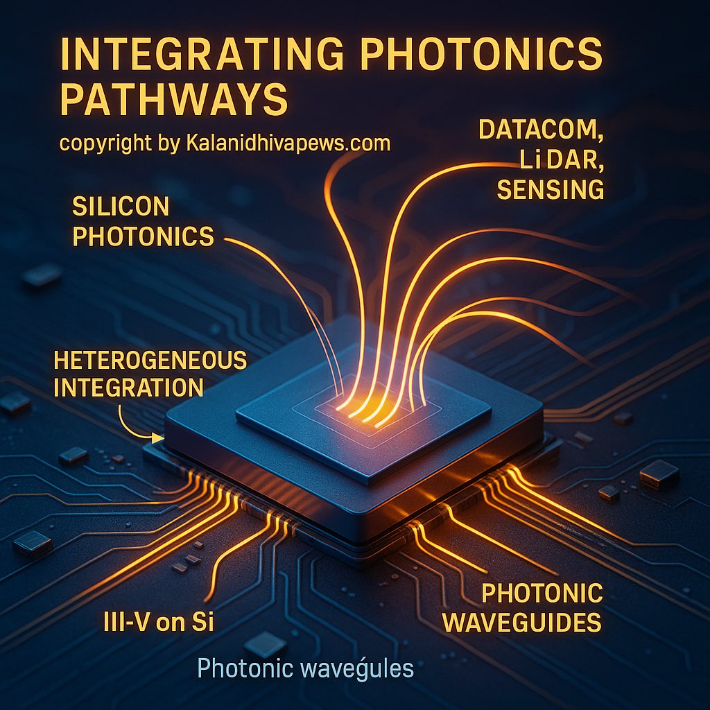
![]() Photonics is transforming microelectronics by enabling faster data transfer, sensing, and communication. Silicon photonics, III-V on Si, and heterogeneous integration combine to create hybrid chips where light and electrons work together. Applications span datacom, LiDAR, and precision sensing, laying the foundation for energy-efficient computing and AI acceleration powered by light-speed interconnects.
Photonics is transforming microelectronics by enabling faster data transfer, sensing, and communication. Silicon photonics, III-V on Si, and heterogeneous integration combine to create hybrid chips where light and electrons work together. Applications span datacom, LiDAR, and precision sensing, laying the foundation for energy-efficient computing and AI acceleration powered by light-speed interconnects.
copyright by www.kalanidhivapinews.com
![]() www.instagram.com/kalanidhivapinews
www.instagram.com/kalanidhivapinews
![]() Manufacturing Next-Gen Chips
Manufacturing Next-Gen Chips
![]() Advanced semiconductor manufacturing combines precision-driven processes to deliver chips at the smallest nodes. Lithography defines circuit patterns, implantation tailors electrical properties, CMP ensures uniformity, and packaging secures the final design. These tightly integrated processes drive performance, efficiency, and reliability in chips powering AI, photonics, and global connectivity.
Advanced semiconductor manufacturing combines precision-driven processes to deliver chips at the smallest nodes. Lithography defines circuit patterns, implantation tailors electrical properties, CMP ensures uniformity, and packaging secures the final design. These tightly integrated processes drive performance, efficiency, and reliability in chips powering AI, photonics, and global connectivity.
copyright by www.kalanidhivapinews.com
![]() www.instagram.com/kalanidhivapinews
www.instagram.com/kalanidhivapinews
#Semiconductors – Materials that conduct electricity under certain conditions, forming the foundation of chips used in computing, communication, and sensing.
#Photonics – The science and technology of light manipulation for communication, sensing, and processing in integrated circuits.
#Microelectronics – A field focused on designing and manufacturing miniature electronic components such as ICs, processors, and memory.
#ChipDesign – The process of creating the architecture and circuit layout of integrated circuits, from logic to physical structures.
#EDA – Electronic Design Automation, the software tools used to design, verify, and optimize integrated circuits.
#SiGe – Silicon-Germanium, a semiconductor alloy used for high-speed, low-power devices and RF integration.
#III-VMaterials – Semiconductor compounds (like GaAs, InP) that enable high-speed electronics and photonic devices.
#2Dmaterials – Ultra-thin atomic materials like graphene and MoS₂ with extraordinary electronic and photonic properties.
#EUVLithography – Extreme Ultraviolet Lithography, an advanced method for patterning ultra-small features on chips.
#ProcessDevelopment – The engineering stage where new semiconductor processes (etch, deposition, annealing) are tested and refined.
#CMP – Chemical Mechanical Planarization, a polishing method that ensures flat wafer surfaces for further processing.
#Etching – A critical step in chip fabrication to remove material and define circuit patterns at the nanoscale.
#Deposition – A process where thin films of materials are layered on wafers to create circuits and interconnects.
#QuantumComputing – A next-generation computing paradigm leveraging quantum states for exponential computational power.
#Neuromorphic – Chip architectures inspired by the human brain to enable energy-efficient AI and adaptive learning systems.
#HeterogeneousIntegration – The combination of different semiconductor technologies (logic, memory, photonics) into one package.
#SiliconPhotonics – Integration of photonic components into silicon chips for high-speed optical communication.
#LiDAR – Light Detection and Ranging, a photonic sensing technology used in autonomous vehicles and mapping.
#DataCom – Short for data communication, covering chip-to-chip and system-level communication enabled by photonics.
#Interconnects – Electrical or optical pathways connecting transistors and circuits within and across chips.
#Packaging – The final stage of chip manufacturing where devices are encased and electrically connected to systems.
#YieldOptimization – Improving the percentage of functional chips per wafer, essential for cost efficiency and reliability.
#Metrology – Measurement science applied in fabs to ensure accuracy, precision, and defect management.
#GlobalFabNetwork – The distributed system of semiconductor foundries, test houses, and packaging plants worldwide.
#SupplyChainResilience – Strategies to ensure continuity of chip production despite geopolitical, material, or logistics risks.
#Standards – Industry frameworks like SEMI, ISO, and JEDEC that ensure interoperability, safety, and global compliance.
#ChipSecurity – Protecting semiconductor IP and manufacturing systems against tampering, espionage, and cyber risks.
#Sustainability – Eco-friendly semiconductor practices including water recycling, energy efficiency, and safe chemicals.
#AIinFabs – Artificial intelligence applications in manufacturing for predictive maintenance, defect detection, and process optimization.
#3DIntegration – Stacking multiple chip layers vertically to achieve higher density, performance, and functionality.


